- 您现在的位置:买卖IC网 > Sheet目录1993 > DS1318E+ (Maxim Integrated Products)IC COUNTER ELAPSED TIME 24-TSSOP
DS1318
Parallel-Interface Elapsed Time Counter
2
_____________________________________________________________________
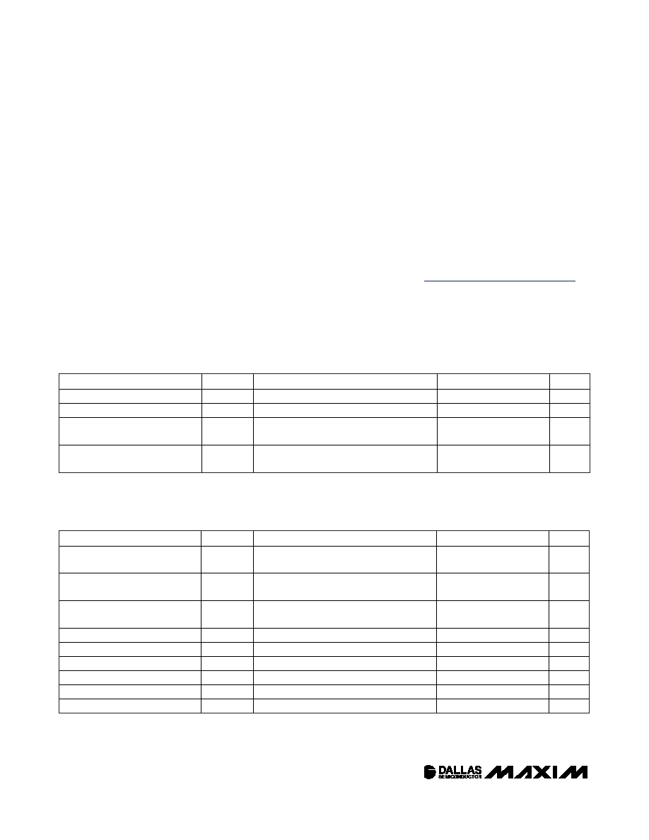
ABSOLUTE MAXIMUM RATINGS
RECOMMENDED DC OPERATING CONDITIONS
(VCC = VCC(MIN) to VCC(MAX), TA = -40°C to +85°C, unless otherwise noted.) (Note 2)
Stresses beyond those listed under “Absolute Maximum Ratings” may cause permanent damage to the device. These are stress ratings only, and functional
operation of the device at these or any other conditions beyond those indicated in the operational sections of the specifications is not implied. Exposure to
absolute maximum rating conditions for extended periods may affect device reliability.
Voltage Range on any Pin Relative to Ground ......-0.3V to +6.0V
Operating Temperature Range ...........................-40°C to +85°C
Storage Temperature Range .............................-55°C to +125°C
Lead Temperature (soldering, 10s) .................................+260°C
Soldering Temperature (reflow) .......................................+260°C
PACKAGE THERMAL CHARACTERISTICS (Note 1)
TSSOP (multilayer board)
Junction-to-Ambient Thermal Resistance (
θJA) ............72°C/W
Junction-to-Case Thermal Resistance (
θJC) .................13°C/W
PARAMETER
SYMBOL
CONDITIONS
MIN
TYP
MAX
UNITS
Supply Voltage
VCC
(Note 3)
3.0
3.3
3.6
V
Battery Voltage
VBAT
(Note 3)
1.6
3.3
3.7
V
Logic 1 Voltage
VIH
(Note 3)
0.7 x
VCC
VCC +
0.5
V
Logic 0 Voltage
VIL
(Note 3)
-0.5
+0.3 x
VCC
V
DC ELECTRICAL CHARACTERISTICS
(VCC = VCC(MIN) to VCC(MAX), TA = -40°C to +85°C, unless otherwise noted.) (Note 2)
PARAMETER
SYMBOL
CONDITIONS
MIN
TYP
MAX
UNITS
Logic 0 Output Current
(VOL = 0.15 x VCC)
IOL
3
mA
Logic 1 Output Current
(VOH = 0.85 x VCC)
IOH
1
mA
SQW, INT Logic 0 Output
(VOL = 0.15 x VCC)
IOLSI
5
mA
Input Leakage
ILI
(Note 4)
1
μA
I/O Leakage
ILO
(Note 5)
-1
+1
μA
Active Supply Current
ICCA
(Note 6)
10
mA
Standby Current
ICCS
(Note 7)
100
150
μA
Battery Input-Leakage Current
IBATLKG
10
100
nA
Power-Fail Voltage
VPF
(Note 3)
2.70
2.97
V
Note 1:
Package thermal resistances were obtained using the method described in JEDEC specification JESD51-7, using a four-
layer board. For detailed information on package thermal considerations, refer to www.maxim-ic.com/thermal-tutorial.
发布紧急采购,3分钟左右您将得到回复。
相关PDF资料
DS1337S+C01
IC RTC SERIAL 2WIRE LP 8-SOIC
DS1338C-33#T&R
IC RTC 56BYTE NV SRAM 16SOIC
DS1339AU+
IC RTC I2C W/ALARM 8USOP
DS1339C-2#
IC RTC I2C W/ALARM 16-SOIC
DS1340Z-33/T&R
IC RTC I2C W/CHARGER 3.3V 8-SOIC
DS1340Z-3
IC RTC I2C W/CHARGER 3V 8-SOIC
DS1341T+
IC RTC I2C W/ALARM 6TDFN-EP
DS1344D-33+
IC RTC SPI 3.3V 14TDFN-EP
相关代理商/技术参数
DS1318E+T&R
制造商:Maxim Integrated Products 功能描述:44 BIT PRLLEL INTFC ETC TRL LF - Tape and Reel 制造商:Maxim Integrated Products 功能描述:IC COUNTER ELAPSED TIME 24TSSOP
DS1318E+T&R
功能描述:实时时钟 PARALLEL-INTERFACE ELAPSED TIME COUNTER RoHS:否 制造商:Microchip Technology 功能:Clock, Calendar. Alarm RTC 总线接口:I2C 日期格式:DW:DM:M:Y 时间格式:HH:MM:SS RTC 存储容量:64 B 电源电压-最大:5.5 V 电源电压-最小:1.8 V 最大工作温度:+ 85 C 最小工作温度: 安装风格:Through Hole 封装 / 箱体:PDIP-8 封装:Tube
DS13-1Y
功能描述:固态继电器-工业安装
RoHS:否 制造商:Crydom 控制电压范围:4 VDC to 32 VDC 负载电压额定值:7 VDC to 72 VDC 负载电流额定值:160 A 触点形式: 输出设备:SSR 安装风格:Panel
DS1321
功能描述:IC CTRLR NV W/BATT MON 5V 16-DIP RoHS:否 类别:集成电路 (IC) >> 存储器 - 控制器 系列:- 标准包装:45 系列:- 控制器类型:静态 RAM(SRAM) 电源电压:4.5 V ~ 5.5 V 工作温度:0°C ~ 70°C 封装/外壳:16-SOIC(0.295",7.50mm 宽) 供应商设备封装:16-SOIC W 包装:管件
DS1321_04
制造商:DALLAS 制造商全称:Dallas Semiconductor 功能描述:Flexible Nonvolatile Controller with Lithium Battery Monitor
DS1321+
功能描述:存储器控制器 Flexible NV Cntlr w/Lithium Battery RoHS:否 制造商:Maxim Integrated
DS1321E
功能描述:IC CTRL NV W/BATT MON 5V 20TSSOP RoHS:否 类别:集成电路 (IC) >> 存储器 - 控制器 系列:- 标准包装:45 系列:- 控制器类型:静态 RAM(SRAM) 电源电压:4.5 V ~ 5.5 V 工作温度:0°C ~ 70°C 封装/外壳:16-SOIC(0.295",7.50mm 宽) 供应商设备封装:16-SOIC W 包装:管件
DS1321E/T&R
制造商:Maxim Integrated Products 功能描述:NV CONTRL 5V X4 BW&RST 20-TSSOP T&R - Tape and Reel 制造商:Maxim Integrated Products 功能描述:IC CTRL NV W/BATT MON 5V 20TSSOP